

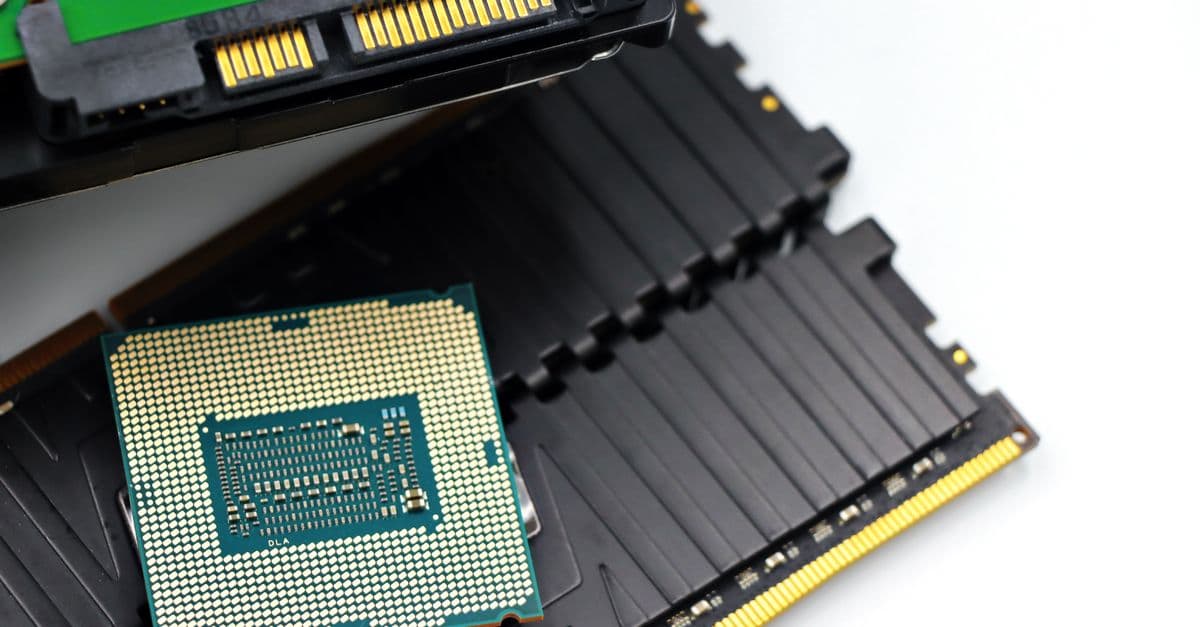
Semiconductor Yield Loss Investigation & Root Cause Analysis
Rapidly investigate semiconductor yield loss and pinpoint process root causes
What You Can Do
You can upload wafer test data, manufacturing logs, and process parameters to quickly identify yield-loss patterns, correlate defects to process conditions, and generate prioritized root cause hypotheses. Claude analyzes multi-dimensional manufacturing data to uncover process bottlenecks, suggest containment actions, and recommend optimization experiments backed by statistical evidence.
Features
Automatically identify spatial and temporal defect clusters across wafer maps, layers, and process batches using statistical clustering and heat map analysis.
Cross-reference yield anomalies with process setpoints (temperature, pressure, duration, materials) to surface process conditions that correlate with loss events.
Synthesize defect data, process logs, and equipment status into ranked root cause hypotheses with evidence scoring and risk assessment.
Apply statistical rigor to validate whether observed yield differences are real or noise, helping you prioritize investigation effort.
Correlate defects across process layers (lithography, etch, deposition) to determine whether root cause is layer-specific or systemic.
Track yield improvement or degradation over time and link trends to equipment maintenance events, process changes, or material lot changes.
Generate containment action plans and design verification experiments to isolate root cause and validate fixes before full-line implementation.
Example Output
Input: Wafer test results (500 wafers), tool parameter logs, and defect classification data.
Output:
- Defect Distribution: 67% metal bridging in M2 layer, clustered in northwest quadrant of wafers processed on Tool_A between 3–5 PM.
- Root Cause Analysis: High probability of CMP over-polish (correlated with Tool_A's slurry feed rate spike on 2026-08-08). Confidence: 84%.
- Recommended Actions: (1) Lower slurry flow rate 15% on Tool_A; (2) Compare CMP film thickness vs. design margin; (3) Run design-of-experiment (DOE) on slurry concentration.
- Verification Plan: Test 50-wafer batch with corrected parameters; expect yield recovery to 98%+ if CMP is root cause.
What's Included
- Yield Loss Investigation Template: Structured framework for collecting data, organizing symptoms, and systematically narrowing root cause search space.
- Defect Classification & Binning Guide: Reference guide for standardizing defect nomenclature and physical binning to align analysis with fab capability and SPC systems.
- Process Correlation Worksheet: Pre-formatted analysis sheet for mapping defect timing/location to process parameter values, material lot codes, and equipment IDs.
- Root Cause Verification Checklist: Systematic checklist to validate hypotheses before implementing fixes, including hypothesis elimination, statistical tests, and DOE design.
- Yield Report Generator: Template for synthesizing findings, recommendations, and next steps into executive-ready briefing slides and engineering documentation.
- Troubleshooting Playbook: Decision tree for common yield-loss scenarios (metal defects, thin film variability, lithography vias, etc.) with typical process culprits.
Who It's For
- Manufacturing Engineers
- Process Engineers
- Yield Engineers
- Quality Assurance Managers
- Production Supervisors
Best For
- Urgent yield loss investigations and containment
- Multi-factor defect root cause isolation
- Process optimization and capability improvement
- Equipment troubleshooting and maintenance planning
- Design-of-experiment planning for process validation
You might also like

You can structure and run Kaizen events from start to finish, guiding your team through waste analysis, root-cause identification, and rapid improvement design. The skill generates detailed event agendas, countermeasure documentation, and performance metrics—enabling you to close improvement opportunities within days rather than weeks.
 by kylezantos
Prepare comprehensive audit documentation and manage ISO 9001/14001 compliance faster. You can generate tailored audit checklists, analyze nonconformance findings systematically, and develop corrective action plans that meet ISO standards — all in hours instead of days. This skill ensures consistent documentation across your manufacturing operations and maintains audit readiness year-round.
by kylezantos
Transform raw manufacturing P&L data into actionable insights by automatically identifying cost variances, pinpointing root causes, and generating executive-ready narratives. You upload your plant's P&L statement, provide context about recent operational changes, and Claude analyzes the numbers to explain why costs moved and what actions drive profitability.
by kylezantos
This skill systematically analyzes out-of-spec chemical manufacturing batches to identify root causes and recommend parameter adjustments. You provide process data, operating conditions, and quality metrics; Claude performs hypothesis testing, statistical correlation analysis, and multi-variate optimization to pinpoint the failure mechanism. You get actionable recommendations ranked by impact and implementation risk.
by kylezantos
You can leverage Claude to streamline every aspect of film production coordination—from managing crew schedules and budgets to troubleshooting on-set logistics and creative challenges. This skill helps you create call sheets, coordinate locations, track production expenses, and quickly solve problems that arise during shooting without disrupting your workflow.
by kylezantos
You provide production data and process details, and this skill systematically analyzes the information to identify root causes of quality issues, yield losses, or equipment failures. It develops prioritized corrective actions with implementation timelines, compliance documentation, and performance metrics to track improvement effectiveness.
by kylezantos
This skill systematically analyzes your production data using proven continuous improvement methodologies like Lean and Six Sigma to identify bottlenecks, root causes, and measurable improvement opportunities. You'll receive prioritized, actionable recommendations with implementation roadmaps and risk assessments that help you focus on high-impact optimizations driving real cost savings and efficiency gains.
by kylezantos
Prepare comprehensive audit documentation, track non-conformance issues from identification through resolution, and generate corrective action plans. You can document audit findings, prioritize risks by severity, assign accountability, and create formal reports that demonstrate compliance readiness to auditors and stakeholders.
by kylezantos