


EMC/EMI Testing and Troubleshooting Assistant
Troubleshoot electromagnetic interference and ensure EMC compliance throughout product development

What You Can Do
You get expert guidance on identifying and resolving electromagnetic compatibility issues in your designs. This skill helps you diagnose EMI sources, optimize shielding and grounding strategies, navigate regulatory requirements, and make data-driven design decisions that reduce testing cycles and ensure first-pass compliance.
Features
Analyze design schematics and test results to pinpoint the root causes of electromagnetic interference, from switching noise to crosstalk to radiated emissions.
Get step-by-step procedures for FCC, CE, and other regulatory standards, including pre-compliance testing strategies to catch issues before formal lab work.
Receive specific recommendations for shield design, grounding topology, plane arrangement, and material selection based on your frequency range and emission levels.
Learn how to use oscilloscopes, spectrum analyzers, and EMI probes effectively to characterize emissions and verify that your fixes work.
Get actionable feedback on trace routing, layer stackup, via placement, component orientation, and signal integrity techniques that reduce EMI at the source.
Follow structured workflows to narrow down issues systematically, whether you are dealing with conducted emissions, radiated emissions, immunity, or susceptibility problems.
Understand what measurement equipment you need for different types of testing and how to use common lab tools for cost-effective pre-compliance assessment.
Example Output
Example 1: EMI Source Analysis
Problem: 48V switching power supply causes FCC Class B failures above 100 MHz.
Root cause identified:
- Primary source: 250 kHz switching frequency and harmonics (500k, 750k, 1M, etc.)
- Coupling path: Parasitic capacitance between primary and secondary windings
- Secondary path: Poor return path for switching current
Recommended fixes (priority order):
- Add ferrite clamp across primary switches (reduces dV/dt, lowers harmonic content)
- Reduce loop area of switching current path by placing return trace adjacent to power trace
- Add shielded coaxial cable from power supply to load, with shield grounded at source end
- Place 1 nF ceramic capacitor across transformer primary-secondary isolation gap
Example 2: Pre-Compliance Test Plan
For a new USB 3.0 peripheral:
- Equipment needed: 1 GHz oscilloscope, USB near-field probe set, ferrite clamp kit
- Test points: USB differential lines, VBUS, GND return path
- Expected results: Common-mode emission under 70 dBµV at 1m by 1 GHz
- Quick verification: Use oscilloscope probe on USB shield braid near connector; if you see >500 mV peak CM noise, shielding is insufficient
Example 3: Shielding Strategy
For high-speed ADC board radiating excessive RF:
- Faraday cage around ADC, oscillator, and analog supplies (copper or mu-metal enclosure)
- Shield grounding: Multi-point connection to main ground plane (spacing <λ/20 at highest frequency)
- Cable shielding: 360-degree shield termination at connector backshell, not pigtail ground
- Frequency-dependent approach: Add 10 nF capacitors for HF; for frequencies below 1 MHz, rely on solid shield and ground plane coupling
What's Included
- EMI Troubleshooting Flowchart: Interactive decision tree to help you systematically isolate whether you have a conducted emission, radiated emission, immunity, or susceptibility problem.
- Compliance Checklist Templates: Pre-formatted checklists for FCC Part 15, CE/EN standards, and IEC 61000 series testing, so you know what to prepare before lab visits.
- Design Review Framework: Structured questions to ask during PCB and schematic review sessions, covering power distribution, return paths, shielding, and grounding.
- Measurement Technique Guide: Best practices for using oscilloscopes, spectrum analyzers, and field probes to accurately characterize emissions without introducing measurement artifacts.
- Common EMI Patterns Database: Quick-reference catalog of typical EMI signatures (switching noise, crosstalk, common-mode radiation, clock harmonics) and their standard fixes.
- Tool and Equipment Selection Guide: Guidance on which measurement tools you need at each development stage and typical cost ranges for entry-level through advanced lab setups.
Who It's For
- Hardware Design Engineers
- EMC Test Lab Engineers
- PCB Design Specialists
- Product Compliance Engineers
- Manufacturing and Quality Engineers
Best For
- Diagnosing unexpected EMI/EMC test failures
- Pre-compliance assessment and rapid iteration
- Optimizing PCB layout for electromagnetic compatibility
- Selecting shielding, grounding, and filtering strategies
- Navigating regulatory requirements and standards
You might also like
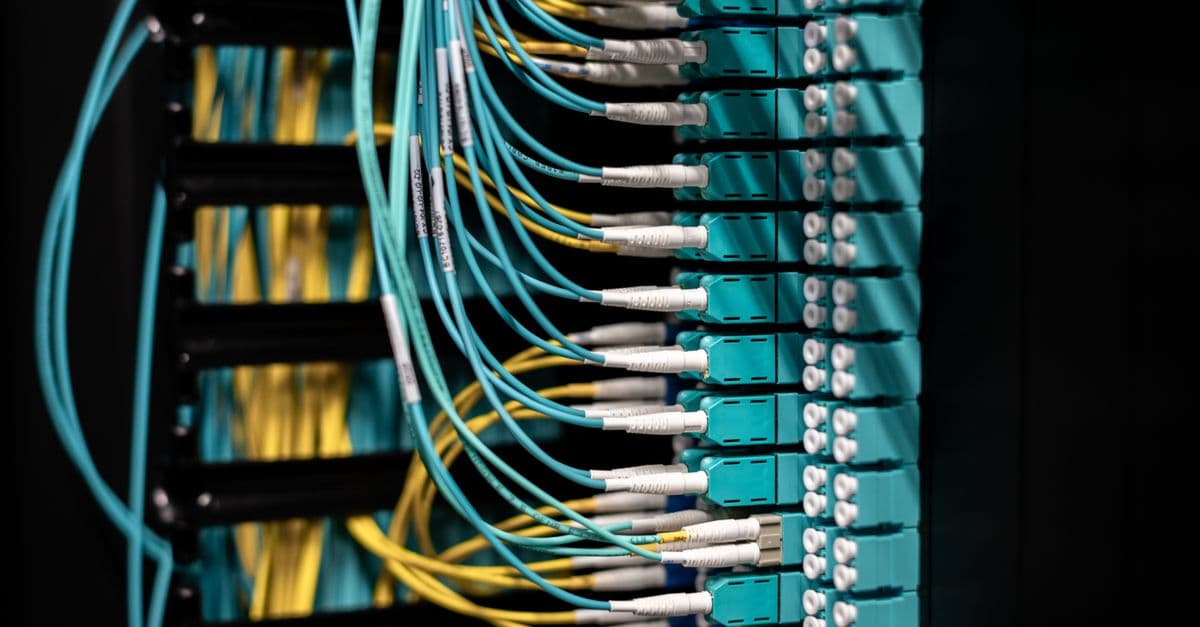
You can upload fiber optic test data (OTDR, reflectance, attenuation measurements) and receive automated analysis with root cause identification, performance metrics, and optimization recommendations. The skill generates professional troubleshooting reports highlighting problem areas, estimated repair costs, and compliance status against industry standards like TIA-942 and IEC 60793.

Systematically analyze your cloud network architecture across security, resilience, cost, and compliance dimensions. You receive a comprehensive assessment report with prioritized optimization recommendations, security hardening steps, and implementation guidance tailored to your infrastructure. The skill evaluates network design patterns, resource utilization, and compliance gaps to help you build cost-effective, secure, and highly available cloud networks.
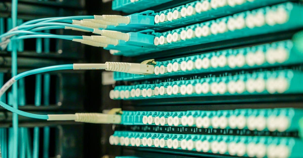
You upload OTDR (Optical Time Domain Reflectometer) test traces or raw test data, and this skill interprets the results to identify fault locations, measure signal degradation, and recommend remediation steps. It accelerates troubleshooting by automating trace analysis and generating professional diagnostic reports that pinpoint connector losses, splice issues, and cable faults with exact distance measurements.

Model how radio waves propagate through environments using empirical and theoretical approaches. Calculate link budgets, predict signal strength at specific locations, and diagnose coverage gaps using measurement data. Claude analyzes your propagation models, suggests optimizations, and interprets measurement results in the context of standard RF theory.

You can design antennas optimized for your specific frequency range and use case, then instantly analyze their predicted performance including gain, radiation patterns, and impedance characteristics. Get actionable recommendations for geometry refinements, matching networks, and feed methods tailored to your constraints. Transform RF design from guesswork into a methodical process with detailed parameter specifications ready for simulation or prototyping.

Calculate complete microwave link budgets including transmit power, antenna gains, path losses, noise figures, and system margins. Analyze RF component performance specifications, verify atmospheric conditions, and predict link availability. Generate structured design documentation with verification checklists and performance recommendations.

This skill assesses electromagnetic compatibility and interference risks in your product design, identifies compliance gaps against international standards (FCC, CE, RoHS), and generates targeted mitigation strategies. You get a structured compliance roadmap with design recommendations, test planning guidance, and regulatory requirements specific to your product category and target markets.
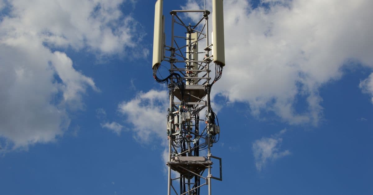
This skill equips you to analyze fiber-to-the-home network architectures, diagnose optical performance problems, and generate comprehensive deployment documentation. You can evaluate network requirements, calculate capacity metrics, identify bottlenecks, and produce professional technical reports that guide installation and optimization efforts.